Micro Cluster Patent Technologies
MLL-1 micro laser line perforation real alternative for galvanometer scanner, cluster micro technology for hole pattern, perforation design, waves, zigzag or packages lines, cryptograms, company logos, holograms, anti counterfeiting, security paper, safety, bank note, metal sticker, printing, laminating, coating, credit cards, transparent films, holographic paper, cigarette, tipping, filter, aluminum foils, shrinkable films, tear tapes, labels, cardboards, bar or matrix codes, marking, scribing, jewelry, automotive, pharmacy, golf, smoking, chemical or medical product, electronics part, indicators, porosity contours or profiles, embossing, bioengineering, membrane, filtration, focus, holographic, hinge-lid, pack, hole, porous, hole, line, micron. Patent pending for process, device, product property DE102004012081.
LPM-1 micro laser perforation at wide web, large area, surface or whole material cluster treatment, cutting, welding, drilling, ablation, cleaning, melding, high power dual rotation laser beam splitter, twin multiplexer level, 4/6KW optical input, flexible hollow fibers, 200 output channels, Co2, Yag, Excimer, UV, emission. Material treatment and robotic handling for stainless steel, ceramic, aluminum, wafer, gold, glass, silver, brass, copper, titanium, diamonds, jewelry, silicon, solar, panel, photovoltaic, micromachining, slitting, rewinding, refining machines or stand along systems. Patent grand for process and device DE102004001327.
Nano Micro perforation or other material including surface treatment, electrostatic nano micro cluster perforation for cigarette, tipping, filter, packaging, plug wrap, Kraft, cement sack, bag, fine and other paper, silicon or other coatings, certain plastic films, laminates, porosity from 80 up to 2500 Coresta Units, from 20 down to 6 Gurley, hole sizes from 50 nm up to 100 microns, hole densities from 80-260 h/cm2, zone widths from 2.0-6.0 mm, up to 16,000,000 holes per Second, web speeds up to 500 m/min, web widths up to 2000 mm. Patent grand DE10328937.
Twin AC/AC, AC/DC frequency shift converter high power, high frequency, high voltage, ultra short mega peak current, electro static nano or micro cluster perforation, ignition, sparking, arc, cigarette, tipping, filter, fine, packaging, paper, plug-wrap, sack, bag, Kraft, food, plastic film, foil, textile, fabrics or other products, switching converter, compressor, emergency, train, ship or vessel power supply, generator, fuel cell, upward, downward, frequency shift switching unit, gas, slab, laser, diode, stack, fiber, beam, material, hybrid, plug-in, car, battery, lithium, Ion, renewable, energy, wind, solar, panel, technology, recycling, medical equipment, membrane filtration, robotic, photovoltaic, industrial automation, drives, IGBT, MOSFET, tube, rf, hv. Patent grand for process and device DE10328937.
Optical online OPSS-1 porovision scanning control system permeability cluster control for electrostatic or laser micro perforation machines, multiple color sensor head, spectral intensity, DSP, FPGA, CCD, line, precise, laser, position, material finger print detection, VIS wave length, opacity, defects, inspection, image control, scanner systems, process software, line, camera, vision control, filter, tipping, cigarette, book, packaging, magazine, bible, wall, Kraft, paper, carton, coffee, tea, food, co-extrusion foils, films, agriculture, cement, domestic or other moving fabrics or web material. Patent pending for process and device DE10251610. China patent grand 200310104764.
In-situ dyne or surface tension control ODSTM-1 at fast moving substrates, plastic, films, foils, tear tape, laminate, co-extrusion, BOPP, LLDPE, PE, PP, PVC, MOV, MOH, FEP, PET, OPP, PTFE, MPET, online, spectral, extinction, monolithic, sensor, analyzing, measurement, wave length, Raman, stray, beaming, water drop, angle, inspection, corona, plasma jet, laser, IR, NIR, scanning, wobbling, stray light, spectrometer, etc. Previous patent application DE19542289.
Patent references http://www.wikipatents.com/gb/2149092.html http://www.wikipatents.com/de/3332886.html http://www.wikipatents.com/de/2918283.html http://www.freepatentsonline.com/EP0460369.html http://www.freepatentsonline.com/7224447.html http://v3.espacenet.com/publicationDetails/biblio?CC=EP&NR=0460369&KC=&FT=E http://www.inpama.com/index.php?content=invention&id=18 http://www.inpama.com/index.php?content=invention&id=19 http://www.inpama.com/index.php?content=invention&id=20 http://www.inpama.com/index.php?content=invention&id=21 http://www.inpama.com/index.php?content=invention&id=22 http://www.inpama.com/index.php?content=invention&id=23 http://www.inpama.com/index.php?content=invention&id=24 https://www.patent-net.de/index.php?content=projekt&id=163 https://www.patent-net.de/index.php?content=projekt&id=213 https://www.patent-net.de/index.php?content=projekt&id=155 https://www.patent-net.de/index.php?content=projekt&id=156 https://www.patent-net.de/index.php?content=projekt&id=214 https://www.patent-net.de/index.php?content=projekt&id=157 https://www.patent-net.de/index.php?content=projekt&id=158 https://www.patent-net.de/index.php?content=projekt&id=287EU technology links
PowerSourcing Links
Nano, micro perforation at running webs
Material webs such as cigarette-, mouthpiece tipping paper, filter-, coated special papers, force papers, bag papers or packing papers, bonded fabrics, spun bonded non-woven, technical textiles, fabrics, laminate, etc. with base weights from 20 g/m2 to up to 150 g/m2, up to 20 g/m2 LPDE coating films, are perforated electro-statically ESP nano micro or laser or mechanical micro or macro for different application purposes.
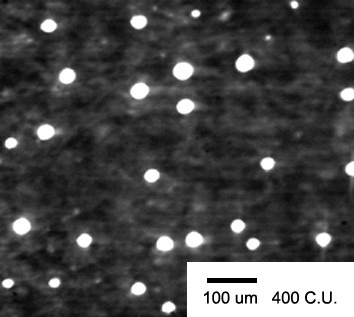
For a better comprehension: Electrostatic NANO MICRO PERFORATION are statistically irregularly distributed, varying by size up to 40 %, and analogically, under LASER or micro/macro mechanical PERFORATION, evenly arranged in diameter about the same in size, at best non-inclined holes und rows of holes of diverse arrangement.
For the human eye invisible electrostatic - ESP nano or micro perforations may be arranged in areas as well as in zones with specific distances within its web. The sizes of the holes range from 1 to 120 µm in diameter and hole sequences from 1.5 to 16 million pores per second. Arrangements of zones are usually carried out in width from 2 to 6 mm and pore density of 15 to 250 pores per cm2 whereas the perforation of areas results in pore densities of up to 2 million pores per m2. ESP perforations allow for porosity levels from 80 to 2500 C. U., width of webs from 100 to 2000 mm at web speeds of up to 500 m/min, depending on the porosity and material consistency in relation to its ability to perforate.


Laser perforation
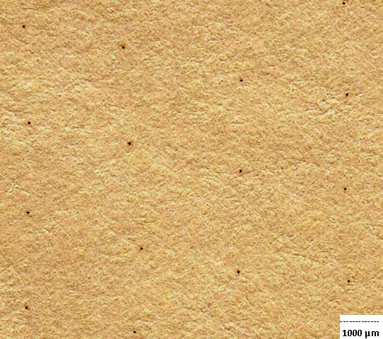
Possible to perforate by pulsed or enlarged and focussed laser beams are hole sizes from 60 to 200 µm at density of holes of typical 10 to 30 holes per cm, hole sequences from 100.000 to 500.000 holes per second at a max. of 32 punctured rows by laser distributed over the width of the web with traditional systems or machine. Their porosity levels range from 100 to 3000 C. U., normally with web widths from 100 to 500 mm at web speeds of up to 600 m/min, depending on the porosity and material consistency in relation to its ability to perforate.
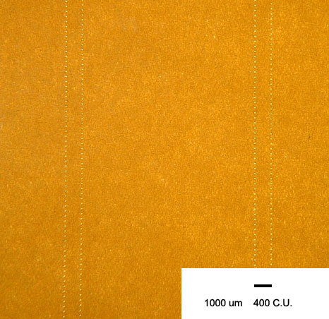
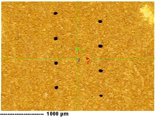
details http://www.microperforation.com/lpm-1.html
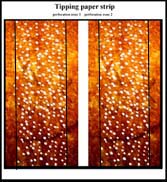
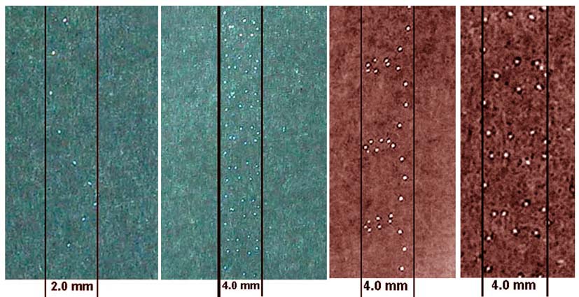
A new patent pending Micro Laser Line perforation technology MLL-1 generates sinus, waves, zigzags or other kinds of perforations designs as multiple pairs of micro laser lines in the web direction. Provide for tipping, cigarette, packaging or other kind of paper webs. These special features of micro laser line perforation enables fundamental new product characteristic in perforation scripts, e.g. for mouthpieces with tipping paper on cigarette filters, products indication with visible perforation holes as brand name or company logo, anti counterfeiting designs, perforation cryptogram, etc. As well is that process to use by other material, industry and application field.
details http://www.microperforation.com/online-perforation-cigarette.html
Perforation of tipping and cigarette paper webs for ventilation of filter cigarettes
The electrostatic ESP perforation has been used more then 25 years for ventilation of non filter or filter cigarettes to create a directed and guided air bypass. For this purpose, cigarette paper for some non filter cigarettes and almost every kind of filter cigarettes tipping papers are perforated electro-statically ESP OFFLINE and in zones from 2.0 6.0 mm width or rows ONLINE or OFFLINE by the use of lasers in order to reduce the harmful substances such as nicotine and condensate down to allowed values. Another effect is the possibility of guiding and controlling the degree of ventilation of the Cigarettes.
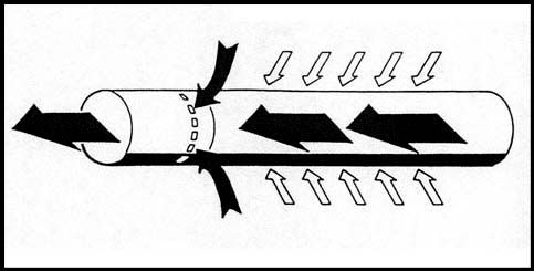
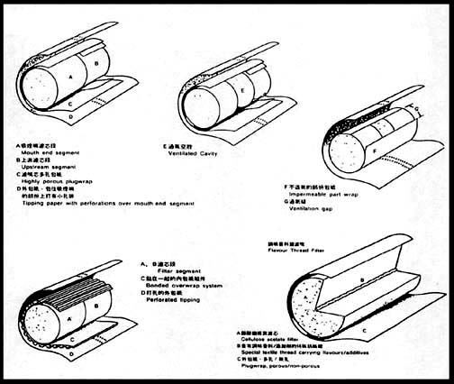
Oder mit fokussierten Laserstrahlen in Offline Verfahren Lochreichenperforationen aber auch im Online Verfahren an der Filteransetzmaschine direkt durch das Mundstückbelagpapierblättchen bis in den Zigarettenfilter gewünschte Poren im Durchmesserbereich von 60 - 120 µm einzubringen, um so Nikotin-, Kondensat- und Schadstoffanteile für den Raucher über die gesteuerte Ventilationskombination auf strikt vorgegebene Werte zu reduzieren.
Vor vielen Jahren hat IPM u.a. auch zur Online Mikroperforation an Zigarettenherstellungsmaschinen ein Verfahren entwickelt und seinerzeit unter EP0460369 sowie DE4018209 zum Patent angemeldet, welche das Einbringen von Mikroperforationsprofilen über die jeweilige Zigarettenlänge sowie in deren Umfang an beliebigen Stellen des Zigarettenpapiers erlaubt.
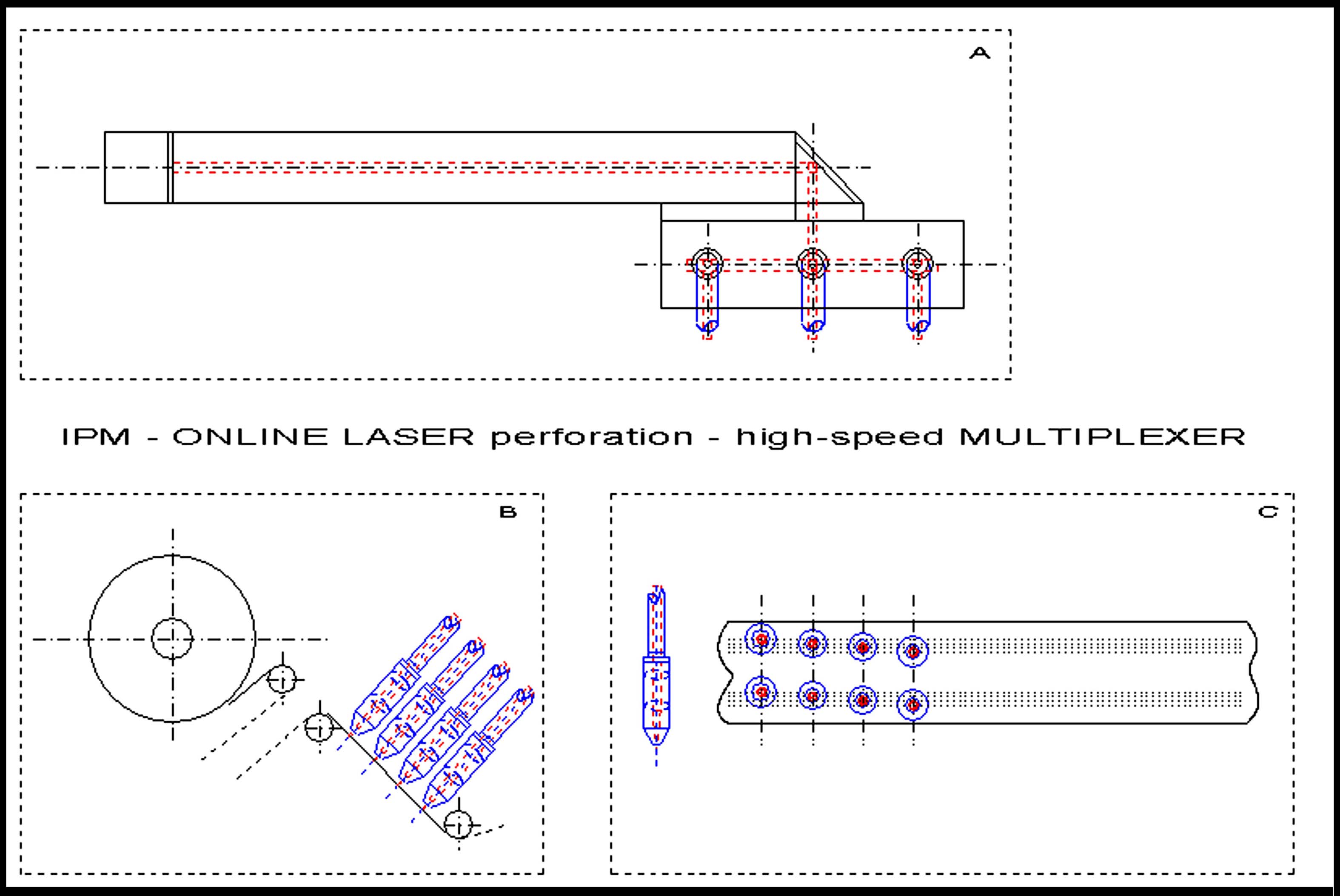
http://www.freepatentsonline.com/EP0460369.html Details http://www.microperforation.com/online-perforation-cigarette.htmlIPM - ONLINE LASER PERFORATION with patent grand high-speed multiplexer DE102004001327
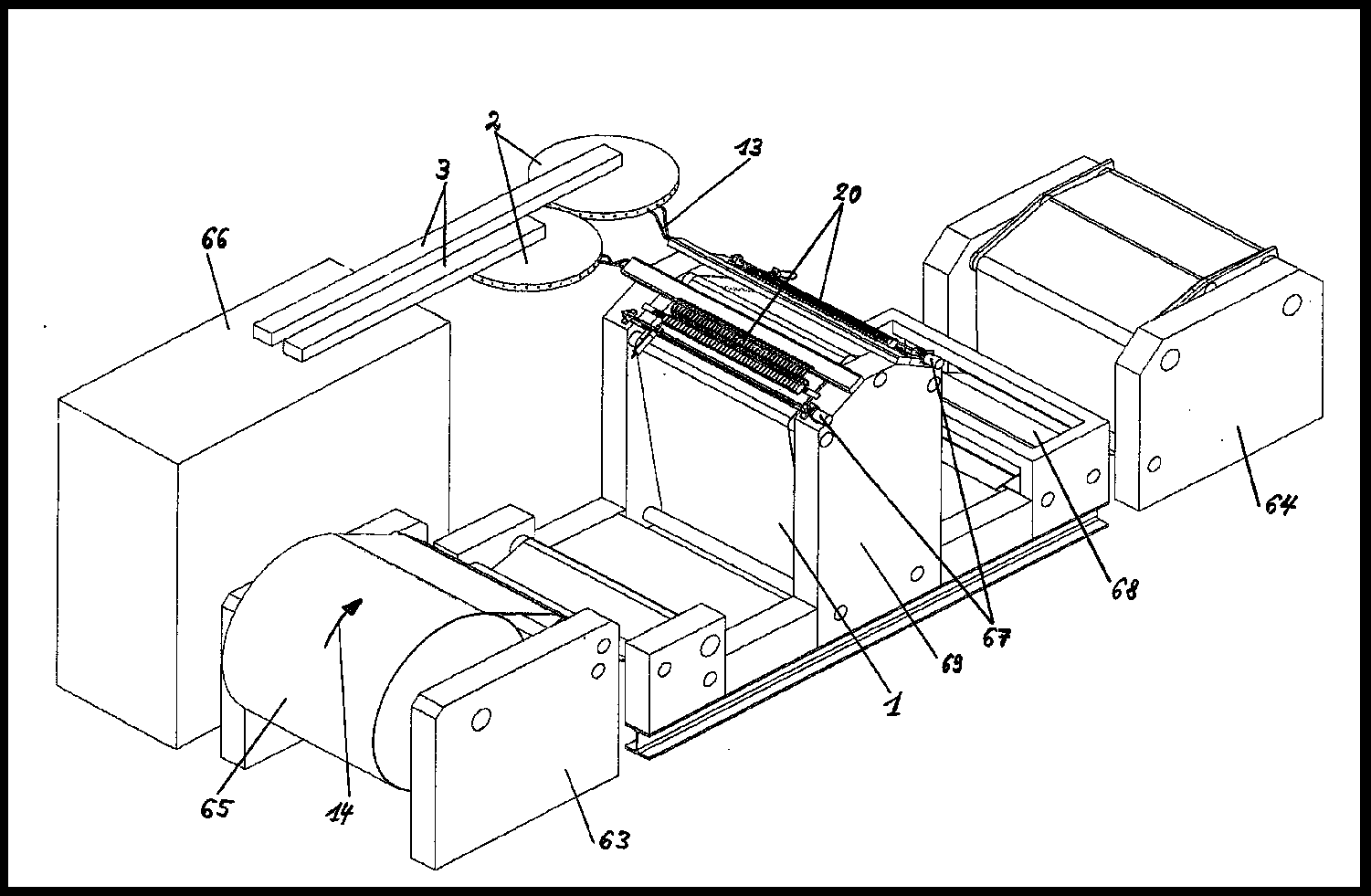
A laser source and IPM patent grand multiplexer with 8 optical channels
B bobbin unwinder and perforation heads
C tipping paper strips with 8 laser perforation lines
further information on request
Special applications and product properties with electrostatic perforation
One of the foremost postulation which can be applied to many application purposes and products containing bonded fabrics, bag- or packaging papers, non-woven, etc. with gas or steam permeability but water impermeability will be found at the application stage of the ELECTROSTATIC NANO/MICRO PERFORATION TECHNOLOGY. Which means pore sizes from 0.5 up to 10 µm diameter by up to 5 million per m2. This is due to the waters greater surface tension which hampers the permeation through the relatively small nano or micro pores. These and other physical advantages of the relatively small pores necessarily demand the application of the ESP perforation method because alternative perforation or processes are NOT feasible, too expensive or simply uneconomical and would not lead to a successful application.
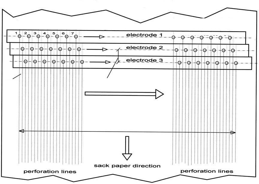
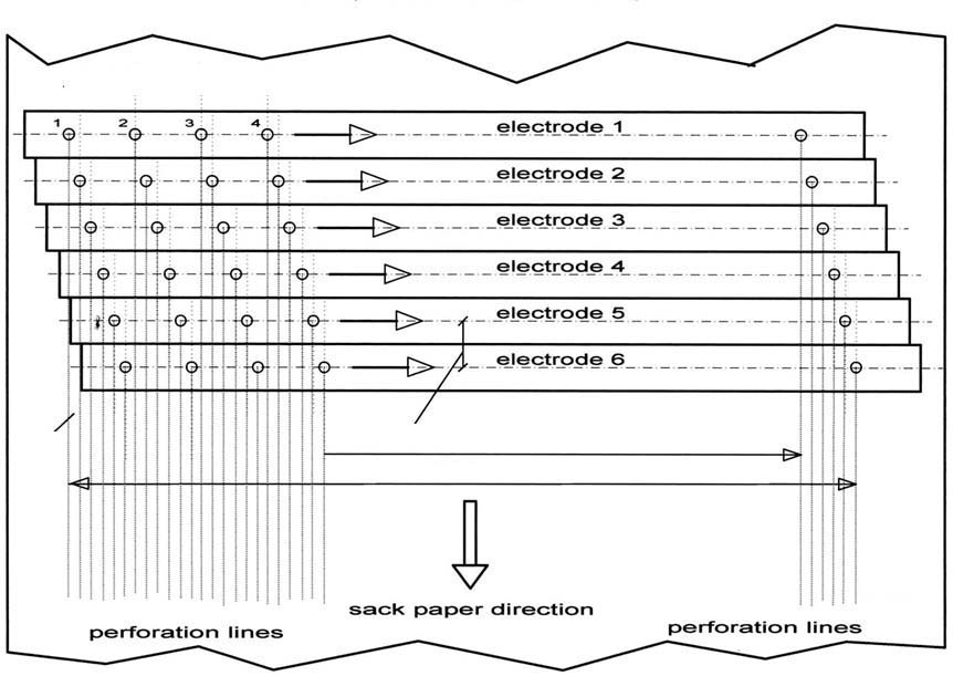
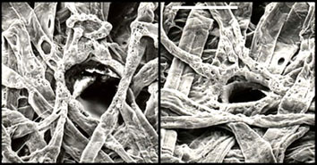
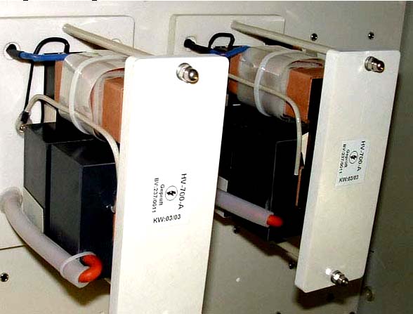
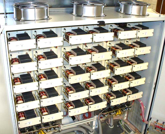
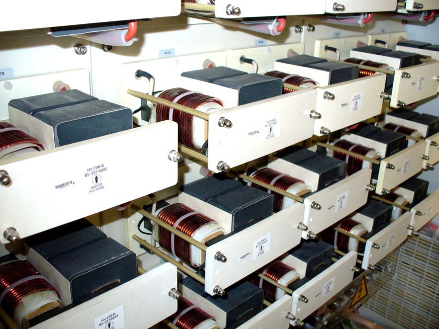
To archive new ESP demands IPM developed/patent grand new electronic perforation circuits which working as upward converters with IGBTs, MOSFET or HVFETs for power pulses from 1 µs up to 25 µs, high current peaks up to 300 Amps, base frequencies up to 200 KHz on ferrite transformers to generate 50 KVss to each sparking electrode.
details http://www.microperforation.com/igbt-esp-unit.html
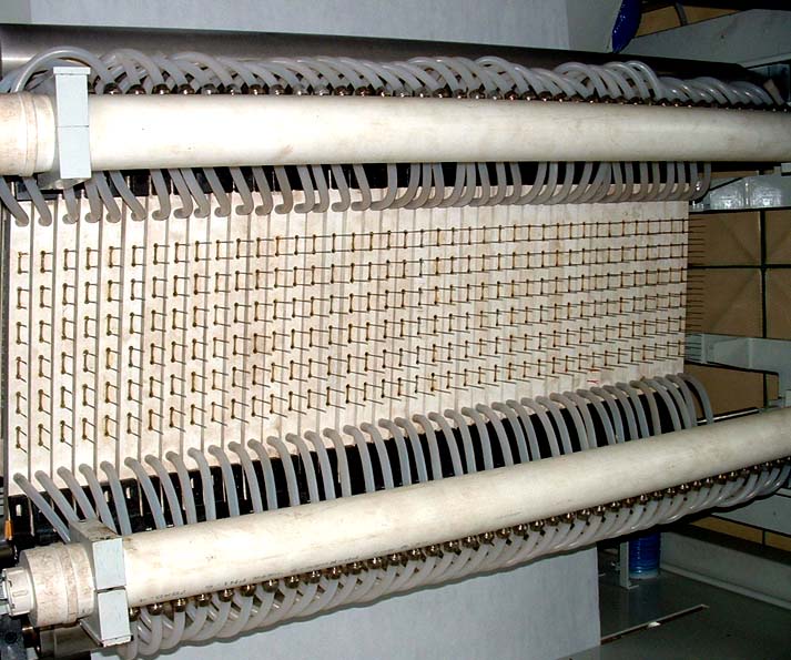
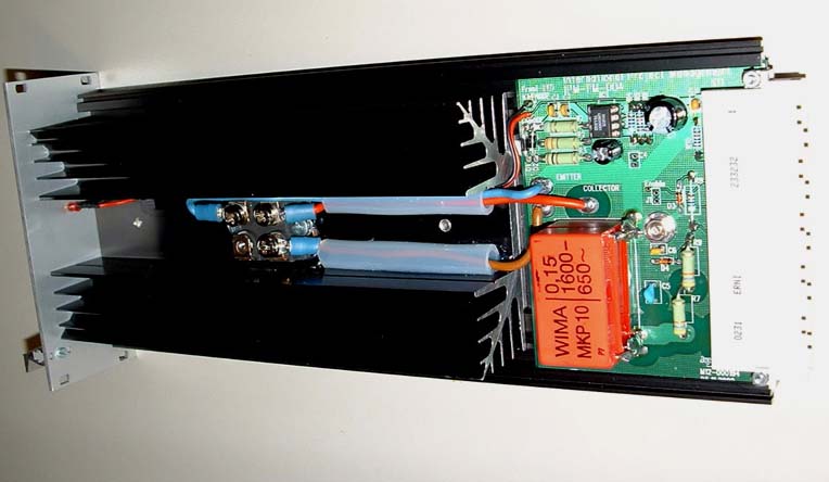
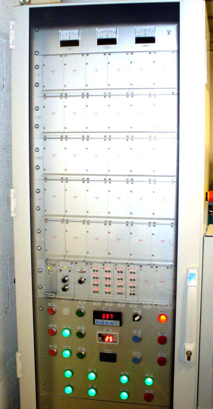
Optical online permeability or porosity vision control
Since naturally porous web materials or web materials to be perforated are processed with speeds of up to 600 m/min and web widths of up to 2000 mm are used, a pneumatic porosity measuring, hence measuring whilst touching the web are highly difficult. Further difficulties of pneumatic measurements are the disadvantages of rising of web tension, material abrasion, folding, leakage at measuring head, impurities, non linear processing and calibration problems.
Thus, optical measuring offers better ways for transmission measuring the pneumatic static permeability for naturally porous or nano, micro or macro perforated webs. The conditions mentioned above can be easily met by using the optical porosity measuring technology thanks to the mentioned product processing and online control, extremely small pore dimensions, relatively high track speeds and a good value repetition.
That full independent from principle material facts as consistence, thickness, weight, colouring, formation, smoothness, brightness, opacity, and other influences.
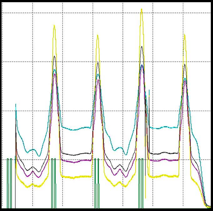
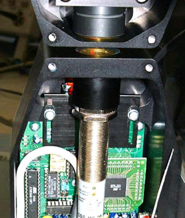

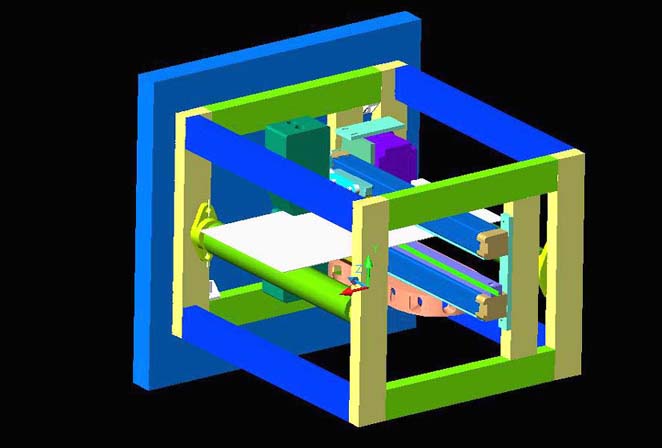
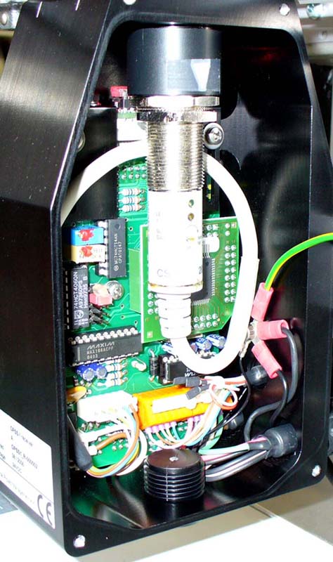
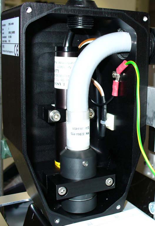
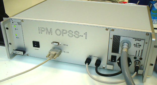
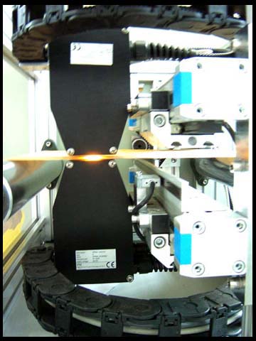
Therefore, IPM International Perforation Management has developed a number of new, patent pending, stationary and transverse optical measurement processes and systems which working with multiple colour sensors, a precision line laser, scanning speeds from 20 200 mm per second, porosity ranges from 80 up to 3000 C.U., perforation lines detection by 0.1 mm, nano/micro holes sizes from 0.5 up to 2000 µm diameter and up to 250 holes/cm2 to determine all data in real time with an internal controller unit in order of multiple light transmissions and perforation profiles to determine envelope curves as well porosity integrals.
details http://www.microperforation.com/opss-1-optical-online-porosity.html
Thus direct feedback into the perforation system makes it possible to compensate any changes in terms of porosity and perforation locations so that each jumbo production roll up to 25,000.00 meters as well single or quadruple bobbin sets can be produced/controlled without intermediate stops and certificated in quantity und quality on their end.
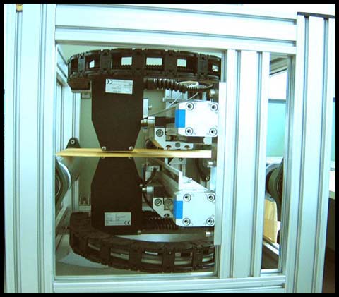
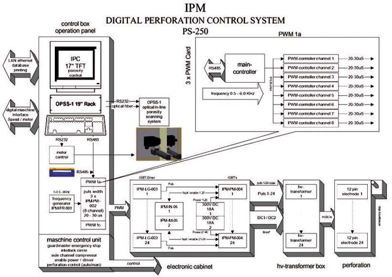
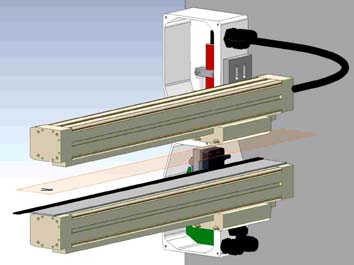
Future prospects
The electrostatic ESP nano or micro perforation usually applies within ranges of the refinement of fine paper, packaging webs, bonded fabrics, non woven, filter paper, bag or force paper as well as special paper webs of most diverse kind especially when additionally treating course materials for achieving special characteristics which for physical or process reasons cannot be achieved by other process technologies.
Our highly modern, industrially approved ESP perforation technology operation which even can be relied on when operated 24/7 can be integrated into existing rewinding course devices or other course devices. Also, they can be used as completely independent perforation devices.
New ranges of applications will be made accessible as new products with special features will be developed.
IPM
International Perforation Management has developed many different kind of
laser or electrostatic perforation processes especially for new product
characteristics. Their devices, systems and machines are in use world-wide.
Introduction
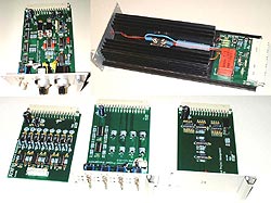
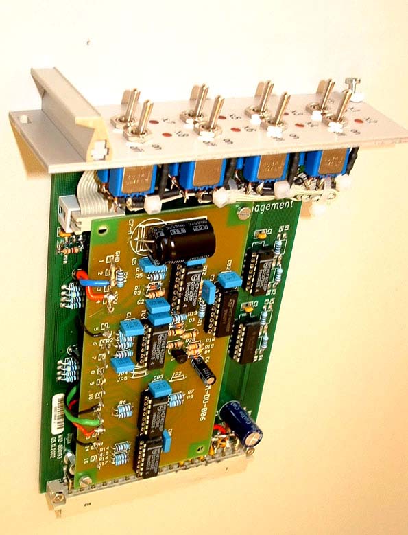
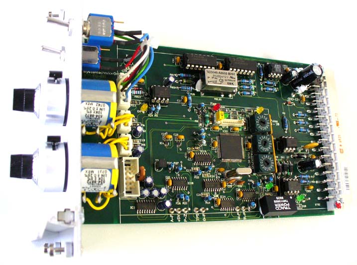
On a high level operate engineering company develops a dual, high power, high frequency switching unit which works with hybrid drives, compact EMI safe semiconductor stages, supporting capacitors, high voltage ferrite transformers to generate HV short pulses and sparking groups. Advantages are based on uses of standard circuits with extended semiconductors for e.g. nano, sub or micro perforation applications, corona treatments etc. The company is looking for science or industrial partners who are interested in a licence agreement and / or technical co-operation.
Working principle
Industry application of electrostatic perforation for fast running paper webs using IGBT, MOSFET or HVFET semiconductor power stages. These circuits working as upward converters with power pulses in ranges from 5 µS up to 25 µS and high current peaks up to 300 Amps on a serial connected inductivity and loading capacity that the secondary ferrite transformer coils supply sparking electrodes up to 50 KVss.
The circuit works itself with alternating clock frequencies and changes of pulse widths a common load condenser and coupled primary inductance of a ferrite high voltage transformer as upward power/pulse converter and non resonance frequency operation.
A safety circuit logic and two hybrid drivers allows a alternately switching of semiconductor A and B which generating higher operation frequencies and power levels meanwhile the electrical and thermal conditions remains on each in the same range as a single switching unit.

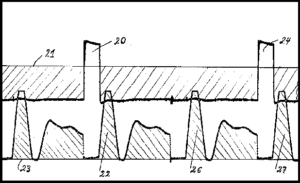
Circuit advantages
A controlled pulse timing into a certain time window with a constant or variable frequency generating hole sizes and hole sequences with high voltage sparking through the material webs by nano or micro perforation. The repeating frequencies of the entire circuit can up to the double switching frequency as of each semiconductor stage.
A changeable current in the spark channel are feasible with total switching frequencies up to 150 kHz. And in the same time the dual semiconductor switching unit allows a double power level as just only with one switching element is possible.
Dual IGBT, HVFET or MOSFET semiconductors in high power, high current, high voltage circuits obtain in electrostatic nano, sub micro perforation, corona treatment or other switching application frequencies up to 250 KHz, power level up to 30 KW and more. Higher power efficiencies and harder switching periods are further advantages.
In conclusion the approximately double frequency and power level operation obtains higher switching efficiencies, much more perforation power or higher corona treatment levels which are depend of the industry application.

Nano Sub Micro Perforation
Perforation results are now achieve for nano, sub and micro perforation of flexible webs with ultra small pores and products made of these materials. Materials finishing are of interest for numerous demands in the field of packaging, in filling, non-woven industry, technical and science applications, etc. For many years fine and other paper webs with base weights between 20 up to 150 g/m2 have been perforated electro statically in large surface all over areas or zone designs of 2.0 6.0 mm width.
Pore sizes from 0.5 µm - 60 µm or 1 to 100 microns, pore distributions of up to 4 Million per m2 in area perforation or respectively 3OO holes per cm2 by zone perforation and hole sequences up to 16 Million per Second can be reached. Air permeability or porosity ranges are among from 50 up to 2,500 C.U. (ml/cm2/min) respectively 3 to 50 l/m2/sec. (Franksystem) by paper web speeds up to 450 m/min and web widths up to 1200 mm are archive able.
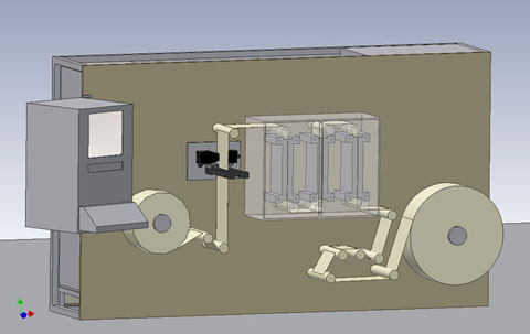
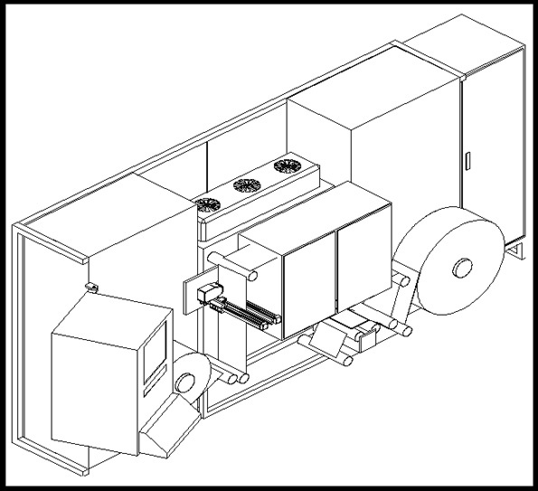
Electrostatic perforation processes and machines, corona treatment, surface treatment, high power switching devices, power supplies, AC&DC and other switching converter systems, drives, etc.
Fine paper, cigarette, packaging or other fine paper industries, corona system manufacture, switching device manufacture, high-power converter equipment, AC/DC, DC/AC industry etc.
The new dual semiconductor circuit design allows applications to build hybrid drives, semiconductor high-level stage, upward, downward or other converters or generators which operating with supporting capacitors, high-voltage ferrite transformers in an extremely compact and modular design. Several advantages are the high efficiency of pulse/power transmission and energy ratios.
Traditional corona or other type of medium generators up to 30 KHz operation ranges are easy to modify to a double frequency and power levels operation.
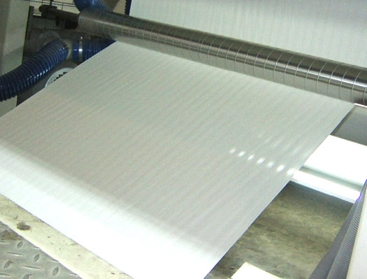
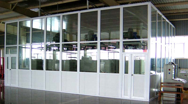
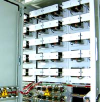
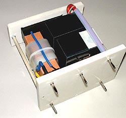
perforation machine PS-1000 - PS-1200 - PS-1600 - PS-2000, PS-250
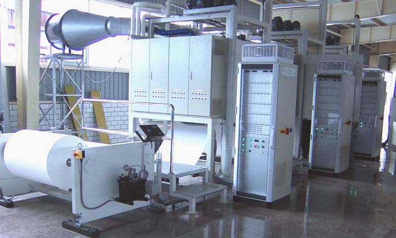
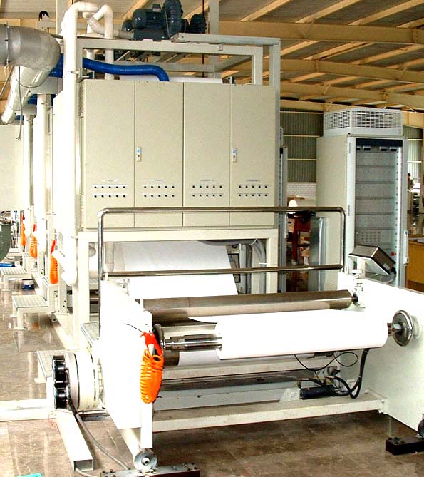
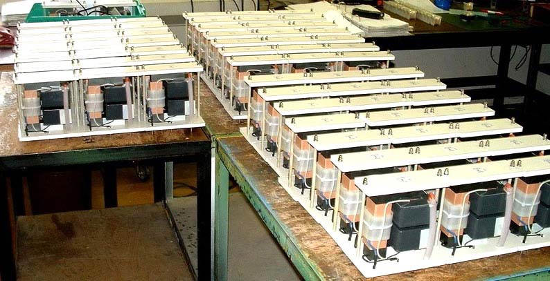
Nano Micro Laser Perforation
High power laser multiplexer for many industry applications as well for LPM-1 wide web micro perforation machines for tipping, packaging paper, non-woven, spun bonded, textile or other material substrates Patent grand DE102004001327
Introduction
A German-Thai-Chinese high-tech engineering company offers completely new possibilities with high power CO2 laser multiplexers for wide web applications as well for micro perforation with JUMBO-ROLLS with up to 200 individual laser perforations rows, automatic laser perforation head positioning, focus setting, web speeds up to 400 m/min, web widths up to 2000 mm and more. Several types of material web, e.g. paper, packaging, coated sheets, films, foils, metal sheets and other types of substrates can be micro perforate or treated. We are seeking for R&D, science or industrial partners in licence agreement, technical cooperation, new product or applications in USA and EU.
Working principle of high-power laser multiplexer
Through 2/4 KW dual laser beam sources, two or four level high-power laser multiplexers designed for certain wave lengths from 500 nm up to 10.6 µm, new two level rotary cubic elements, or two quadruple beam splitters or polygons bent facets, using of new developed CO2 hollow waveguide fibres realizable up to 200 optical single channels with assembled focus heads direct on the production web material. Without very extravagant, expensive of optical elements, alignments, lenses, divert mirrors, extended mechanical designs, etc.
Pulses sequences up to 4,000,000 per second, single shoots between 0.5 up 3.0 mJ, time windows from 1 µs up to 100 µs and e.g. holes sizes from 1 µm up to 100 µm or microns are possible.
Description of wide web micro laser perforation
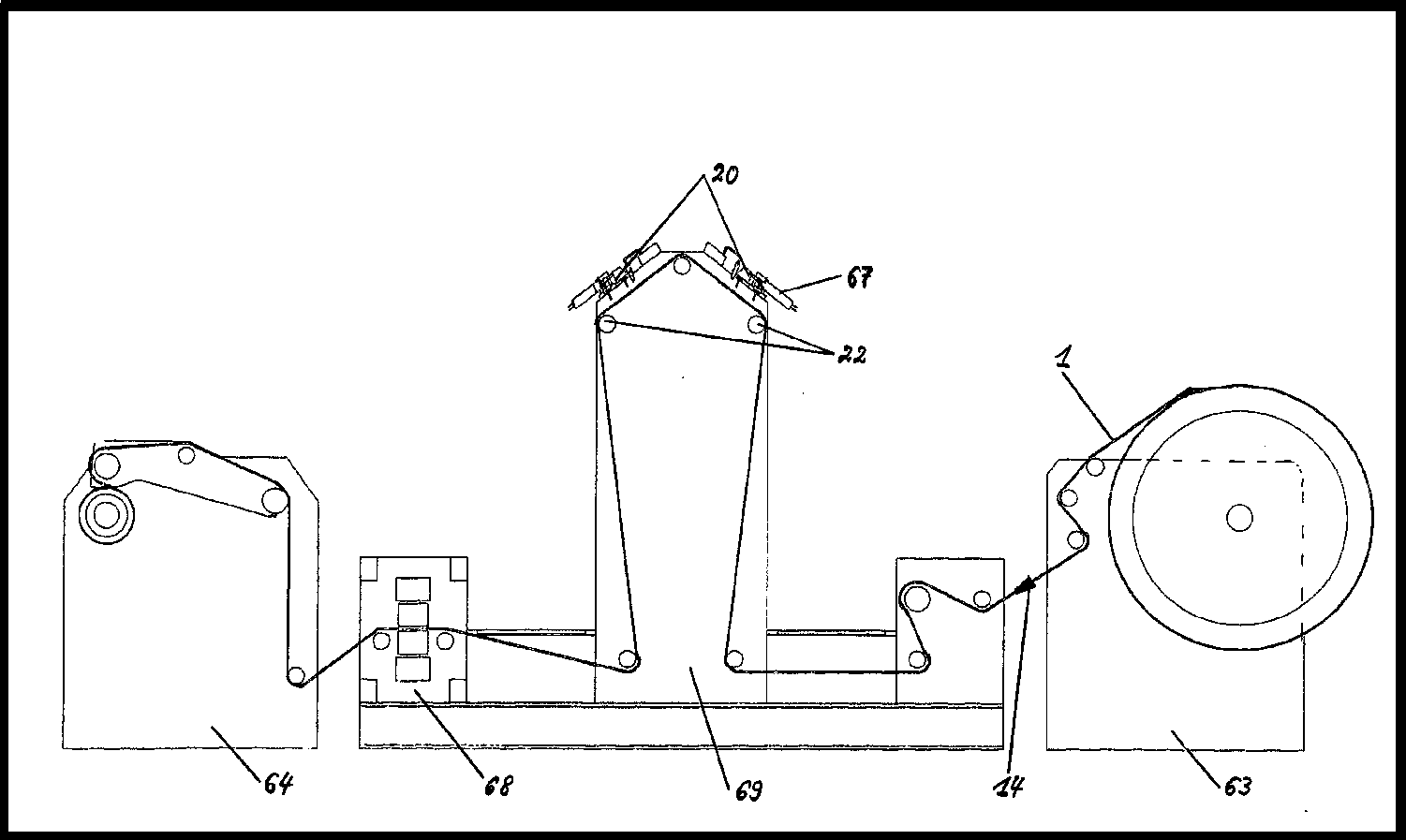
Wide web laser perforation processes, equipment and machines permits e.g. tipping or packaging paper web width up to 2000 mm and more, up to 200 single laser rows across the web by holes sequences up to 4,000,000 per second. Depends of material consistence, perforability, holes sizes and densities web speeds up to 400 m/min, web widths up to 2000 mm, 25,000 meter roll-by-roll, automatic perforation head positioning and focus control, up to 20 bobbins in one cut which means up to 160 bobbins are now archive able without machine downtime. In addition the key element and integrated OPSS-1 porosity/position scanning system complete the feed-back and robot control system. The optical online multi sensor porosity/position control system OPSS-1 is located just behind the laser perforation section and rewind stand to control the perforated material web continuously and supply the data stream to the master PC and close loop.
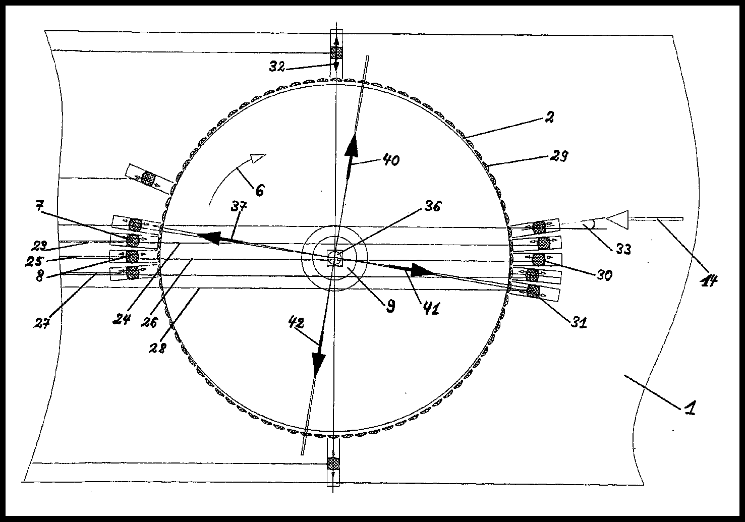

Highly automated and motor adjustable focusing optics one each perforation heads are free position able across the material webs. That automatic procedure and their robot devices open now fully new ways in wide web laser perforations or other material treatments in high speeds ranges, large number of optical single channels and high pulses or holes sequences.
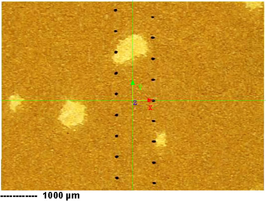

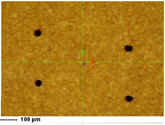
In addition with the optical online control systems OPSS-1 porosity, hole qualities and all hole row positions are continuously controlled and differences immediately compensate over master PC controlled feedbacks to the perforation system. Production rolls and products are finished without intermediate stops in high qualities and large quantities.
Other applications
The new high power laser beam multiplexer open many other application fields, e.g. cutting, cut-offs, welding, surface finishing, drilling, polishing, forming, surface treatment, roughness improvement, etc.
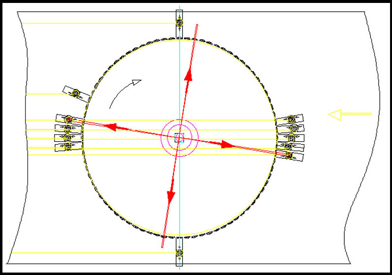
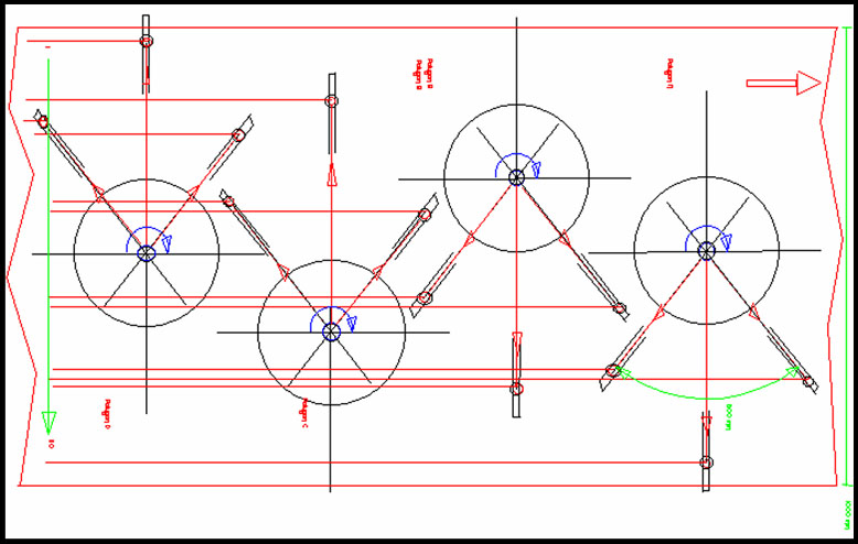
Each of the 200 single perforation head can be positioned across the running web or static positioned material substrate. This automatic processes, equipments and devises open up completely new possibilities in industry, science or military or space laser applications.
Introduction
The German-Thai-Chinese engineering company offers an innovative type of NANO and MICRO LASER LINE PERFORATION technology - that is world wide new. That type of perforation for web, sheet or substrate materials allows a high level of freedom in holes positioning with a variety of perforation designs as wave shapes, zigzag lines etc.
The special characteristics of the technology create fundamentally new product properties. It is adaptable to existing systems. They are looking for industrial partners of license agreements and/or technical co-operation.
Description
Conventional off line laser perforation machines and processes generating straight hole lines in the web direction of the cigarette tipping paper as coaxial shape - or other material sheets. The exception is spray laser designs with randomly distributed holes in certain zones such as electrostatic perforation.
The new
nano micro laser line perforation technology generates sinus, waves, zigzags or
other kinds of lines of perforations hole in web direction as pairs of micro
laser lines.
Tipping paper is the paper around the cigarette filter.
Various new elements move each single laser beam in a sideways direction.

Details
http://www.microperforation.com/mll-1-laser-perforation.html
Product and
process advantages
Existing and new laser perforation machines/systems